Why NVIDIA Is Becoming More Optical: The Second Growth Curve of AI Infrastructure
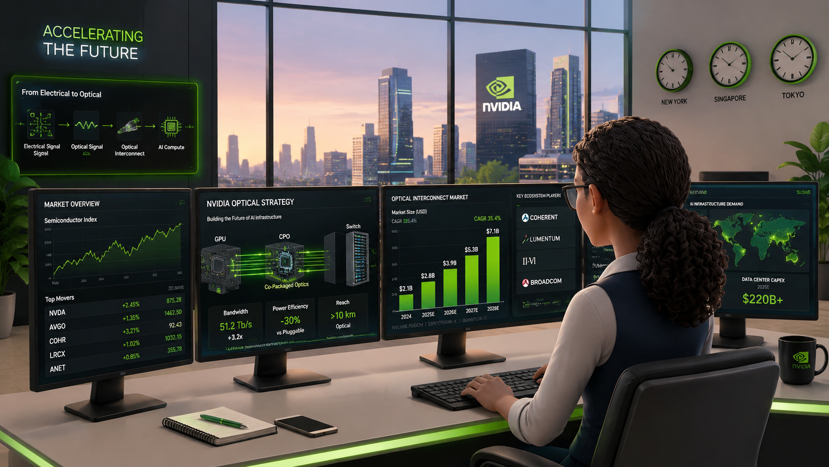
Back in 2023, we wrote about NVIDIA’s transformation from a gaming-GPU company into the most important infrastructure supplier of the generative-AI era. At the time, Amazon, Google, Meta, Microsoft and Oracle were racing to deploy NVIDIA HGX systems, and demand for the H100 far outstripped supply. Our core call was simple: generative AI would kick off a multi-year infrastructure build-out, and with accelerated computing and the CUDA ecosystem, NVIDIA would sit at the center of that capex cycle. (Previous piece: please refer to The Heartbeat of Artificial Intelligence — A Quiet Roar)
Three years on, that call has been thoroughly validated. NVIDIA has become one of the defining infrastructure companies of the AI era, and its product cycles and earnings now move the entire semiconductor and AI-hardware complex. But the story did not stop there. We argued then that NVIDIA was evolving from a GPU company into a full-stack accelerated-computing platform; that transition has now gone one step further — NVIDIA is no longer scaling individual chips or servers. It is scaling entire AI factories. The question this note answers: as compute scales from 8-GPU servers to 72-GPU racks and eventually million-GPU AI factories, where is the bottleneck moving — and why does the answer point to networking, and ultimately to optics?
A New Era: From Training ChatGPT to Agentic AI and Inference
The AI workload itself has changed. In 2023, the conversation was about training ever-larger large language models(LLM). Today, AI infrastructure must support not only pre-training but also post-training, reasoning, long-context inference, and — increasingly — agentic AI, where models continuously plan, call tools, retrieve data and complete multi-step tasks.
The economics of AI infrastructure have changed accordingly. The goal is no longer peak FLOPS(how many calculations a chip can do per second), but maximizing effective token throughput within a fixed budget of capital and power, while driving down cost per token, latency and energy consumption. NVIDIA’s latest Blackwell Ultra and Vera Rubin platforms are designed precisely around this shift.
Looking further out, the ultimate game is Physical AI — models that perceive, reason and act in the real world through robots, autonomous vehicles and automated factories. Training these systems requires simulating the physical world at massive scale; deploying them requires continuous, low-latency inference running around the clock. Each step in this evolution, from chatbot to agent to robot, makes the workload more continuous, more interactive, and dramatically hungrier for compute, memory and bandwidth. Infrastructure built for training a model once is giving way to infrastructure that runs intelligence all the time.
From GPU Scaling to System Scaling
The biggest change since 2023 is that NVIDIA no longer scales just the GPU, or even the server — it scales the entire system. It is also why NVIDIA's product names have become a small test of devotion: B200, GB200, DGX, HGX — if you have ever stared at the lineup wondering whether these are products or license plates, you are not alone. The truth is simpler than the alphabet suggests: one architecture, wrapped and re-wrapped into multiple product tiers. Take Blackwell as an example:
• Blackwell = the architecture
• B200 = the GPU
• Grace Blackwell Superchip = Grace CPU + Blackwell GPU
• GB200 NVL72 = a rack-scale system of 72 Blackwell GPUs + 36 Grace CPUs + NVLink switches
• DGX GB200 = the complete enterprise system NVIDIA sells directly
• HGX Blackwell = the compute platform supplied to OEMs
This could be daunting. What matters is not memorizing the names, but seeing the trend: the basic unit of AI compute keeps expanding, from chip to server to rack to AI factory. GB200 and GB300 NVL72 already fuse 72 GPUs into one unified compute domain over NVLink, and the Rubin roadmap pushes that domain toward multiple racks and hundreds — eventually thousands — of GPUs.
NVIDIA’s Products Now Form a Complete Six-Layer Stack
Reorganized by function, NVIDIA’s product line today forms six layers:
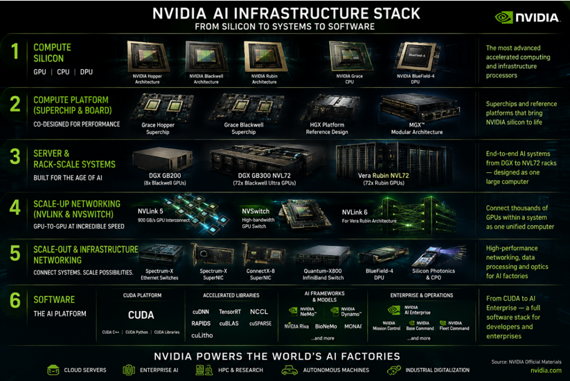
Layer 1: Compute silicon. GPU + CPU + DPU. The GPU does the AI computation; the Grace/Vera CPU handles general-purpose compute and system control; the BlueField DPU offloads networking, storage and security.
Layer 2: Compute platform. Superchips, boards, HGX/MGX. These combine GPUs, CPUs and NVSwitch parts into standard building blocks for servers — Grace Hopper Superchip, Grace Blackwell Superchip, HGX.
Layer 3: Servers and rack-scale systems. DGX, GB200/GB300 NVL72, Vera Rubin NVL72. NVIDIA has moved from 8-GPU servers to 72-GPU racks, engineering the entire rack as one large computer.
Layer 4: Scale-up networking. NVLink + NVSwitch — the high-speed GPU-to-GPU fabric that binds the tens of GPUs inside one compute domain into a single large workload.
Layer 5: Scale-out and infrastructure networking. Spectrum-X Ethernet, Quantum InfiniBand, ConnectX/SuperNICs, BlueField, plus silicon photonics and co-packaged optics (CPO). This layer stitches servers, racks and clusters together and handles data movement, storage and network infrastructure across the data center.
Layer 6: Software. From CUDA to libraries to AI frameworks and inference software to enterprise and infrastructure management — from “making the GPU programmable” all the way to “making the whole AI factory deployable and operable.”
Picture the six layers as a symphony orchestra. GPUs are the musicians (star soloists commanding astronomical fees!); the CPU is the conductor, playing nothing yet deciding who comes in and when (layer one). Musicians form sections (layer two), and sections take the stage as a 72-piece ensemble (layer three: one rack, one orchestra). NVLink is the players hearing one another — a symphony works only when all seventy-two stay on one beat. Let the cellos fall half a beat behind, and the whole orchestra sits there waiting, astronomical fees burning away in the awkward silence (layer four). When a work outgrows one ensemble, several orchestras play it together from different halls, kept in millisecond lockstep by fiber (layer five). And what makes it all possible is the score and its notation: CUDA is the notation every player can read (layer six).
NVIDIA has never been selling a violin. It sells the orchestra, the hall, and the notation itself. Note that two of the six layers — four and five — are about one and the same thing: how the musicians hear one another. That is networking. It is no coincidence, and it is the thread of everything that follows.
Networking: From Peripheral to Core Compute Resource
System scaling created a new bottleneck. A GPU’s value is not just how fast it computes: in large AI models, thousands of GPUs must constantly exchange parameters, activations and intermediate results. When compute improves faster than data movement, GPUs spend more time waiting for data — and adding GPUs no longer adds proportional effective compute.
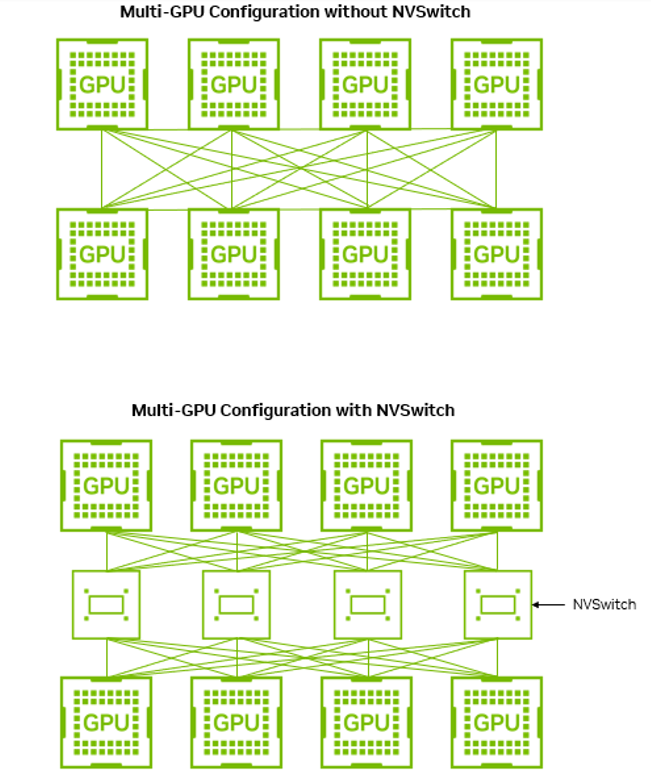
Networking has therefore stopped being an accessory and become part of the computer itself. For an AI factory, the real question is how to keep these increasingly expensive GPUs fed with data and running at high utilization. Good multi-GPU scaling requires outstanding interconnect bandwidth per GPU, plus fast any-to-any paths so every GPU can exchange data with every other GPU as quickly as possible.
The most intuitive example: an NVL72 rack holds 72 GPUs. If each worked independently, the 72nd GPU would simply add one more unit of compute. But large models force these GPUs to trade data constantly — if GPU A finishes its computation but must wait for GPU B’s results, GPU A sits idle and expensive compute is wasted. Blackwell’s fifth-generation NVLink gives each GPU up to 1.8 TB/s of bidirectional bandwidth, and NVSwitch fuses all 72 GPUs into one unified domain.
The engineering metrics have shifted accordingly: training is measured by MFU (model FLOPs utilization), inference by memory-bandwidth utilization, and operations by tokens produced per megawatt. In practice, large training clusters often run at only 30–50% MFU — and much of the lost half is spent waiting on the network. Networking now directly determines GPU utilization and token economics: it accounts for roughly 10–15% of rack cost, yet it gates the productivity of the other 85% of the assets.
The change is already visible in the financials. Before NVIDIA changed its disclosure, Data Center Networking revenue reached a record $14.8 billion in FY2027 Q1, up 199% year-on-year and 35% quarter-on-quarter — growing clearly faster than Data Center Compute. NVIDIA has since stopped reporting networking separately under the old definition, but the trend remains unmistakable: in the latest FY2027 Q2, total revenue reached $96.2 billion, with Data Center revenue of $89.0 billion, up 117% year-on-year, driven by the ramp of Blackwell Ultra infrastructure. Networking is no longer a small attachment to GPU sales — it is an ever-larger pool of value forming around every accelerator.
Optics Enters NVIDIA’s Own Core Roadmap
The Hopper → Blackwell → Rubin roadmap makes the trend explicit. Hopper’s fourth-generation NVLink offered roughly 900 GB/s per GPU; Blackwell’s fifth generation doubled that to 1.8 TB/s; Rubin’s NVLink 6 doubles it again to roughly 3.6 TB/s. Meanwhile the scale-up domain has grown from the traditional 8-GPU server to the 72-GPU rack, and is now extending across multiple racks. Each GPU generation is not only more powerful, it is more communication-intensive. Bandwidth demand has become a second product axis, growing alongside compute.
Structural shift one: scale-out is already optical; scale-up is the next frontier. Scale-out — the links between servers, racks and clusters — already runs largely on optical transceivers and fiber because of the distances involved. Scale-up has historically stayed inside the server or rack, where copper wins on cost, latency and power. But as GPU domains cross the rack boundary, two curves are converging: signaling rates keep rising, which shortens the distance electrical signals can travel reliably, while cluster scale keeps growing, which lengthens the distances that must be covered. Longer distances, shorter copper reach — the lines must cross. The industry debate has accordingly shifted from whether optics enters scale-up to when. Research points to multi-rack architectures, I/O power and bandwidth density as the three main drivers of optical penetration from here.
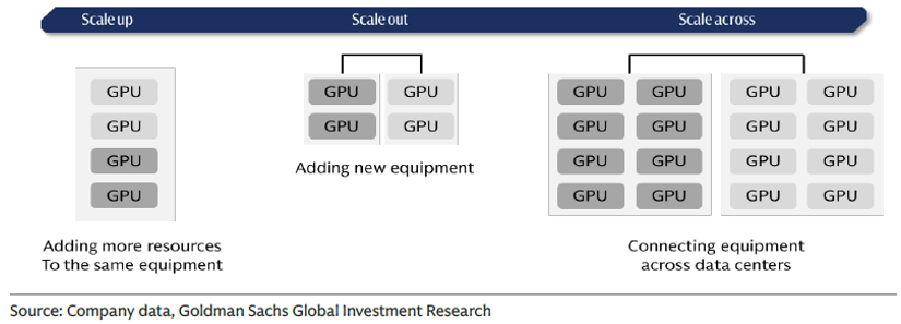
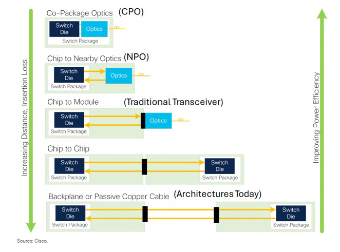
Structural shift two: from pluggables to silicon photonics and CPO — optics is moving closer to the silicon. In the traditional pluggable architecture, a high-speed electrical signal leaves the switch ASIC, travels tens of centimeters across the PCB to a front-panel module, is repaired by a DSP (Digital Signal Processor), and only then becomes light. As per-lane speeds rise, the power and signal-integrity cost of that electrical journey grows steadily worse. Co-packaged optics (CPO) moves the optical engine next to the switch silicon, shrinking the electrical path from tens of centimeters to millimeters. NVIDIA’s Spectrum-X Ethernet Photonics has adopted this approach and entered production; the company cites roughly 5x better network power efficiency versus traditional pluggable networks and positions it as a foundational technology for future million-GPU AI factories.
The Core Framework: Optical Content per GPU
This brings us to the central framework of this note. The traditional approach to optical research starts by forecasting transceiver shipments. We believe the better starting point is the GPU itself. With every GPU generation, ask: how much network bandwidth does each GPU need? How many network ports? How many optical links? How much fiber? How many lasers and optical engines? In short:
Optical TAM = number of GPUs × optical content per GPU
The investment implication is significant. If GPU shipments grow 30% and per-GPU network requirements stay unchanged, optical demand grows roughly 30% as well. But that is not what is happening: bandwidth per GPU is rising rapidly, scale-out port speeds keep upgrading, and scale-up links that are electrical today may progressively convert to optics. Optics therefore carries a second growth multiplier — the opportunity comes not only from more GPUs, but from more connectivity per GPU.
How large is the multiplier? Synthesizing estimates from major sell-side research and industry trackers gives several orders of magnitude:
First, speed migration raises value per port. As GPU uplinks move from 800G to 1.6T on the same three-tier network, the transceiver attach rate roughly doubles from about 3 to about 6 modules per GPU — and each speed step (800G → 1.6T → 3.2T) roughly doubles the module ASP. Volume and price rise together: the first multiplier.
Second, optics entering scale-up opens a new order of magnitude. Measured in optical engines per GPU: about 2 today (all in scale-out); around 17 in multi-rack hybrid architectures (such as Rubin Ultra NVL576, copper inside the rack and optics between racks); and 35 to 70 in a fully optical scale-up. On the same basis, fiber content per GPU rises by a factor approaching 50 — the cross-rack NVLink domain replaces thousands of copper cables one-for-one with fiber.
Third, in dollar terms. Research estimates put optical content per GPU at roughly $2,400 in the GB300 generation, rising to roughly $13,000 in the Rubin Ultra multi-rack generation — more than a five-fold increase, far outpacing GPU unit growth over the same period. That is the second multiplier, quantified.
Investment Implications: Follow the Content, Not Just the Module
For investors, this reframes how to study the optical supply chain. The most visible beneficiaries of 800G and 1.6T have been the transceiver makers, but over time the value migration is likely to be much broader. Rising optical content per GPU pulls through demand for high-power CW lasers, InP, silicon photonics, fiber array units, fiber, advanced packaging and testing.
One further fact is often overlooked: profit is not evenly distributed along this chain. The closer to chips and materials — DSPs, lasers — the higher the margins and the more concentrated the market; assembly is the thinnest-margin, most contested segment. “Rising optical content” therefore does not lift every component equally: LPO and CPO, for instance, are explicitly designed to remove some of the DSP content in traditional pluggables, and when CPO displaces a pluggable port, the “module” line item is partially rewritten as “optical engine + external laser source + fiber.” We need to figure as optics moves closer to compute, which components gain content value and which lose it? Selecting segments along that question tracks the true flow of value better than counting module shipments.
Conclusion: The Next NVIDIA Scaling Story Is About Connectivity
Three years ago, NVIDIA’s story was the scarcity of GPU compute. Compute is still scarce today, but the bottleneck is spreading into more of the infrastructure. NVIDIA is scaling from chip to rack and from rack to AI factory, while AI workloads move from one-off training into continuous reasoning and agentic AI. Every step up in scale means more data movement.
Networking has become part of the machine itself, and optics is closing in on the silicon. The defining metric of the next phase is connectivity per GPU: every new generation ships with more bandwidth, more ports, more fiber and more lasers wrapped around each accelerator. NVIDIA is becoming more optical for a simple reason: light is the only way it can keep scaling.

